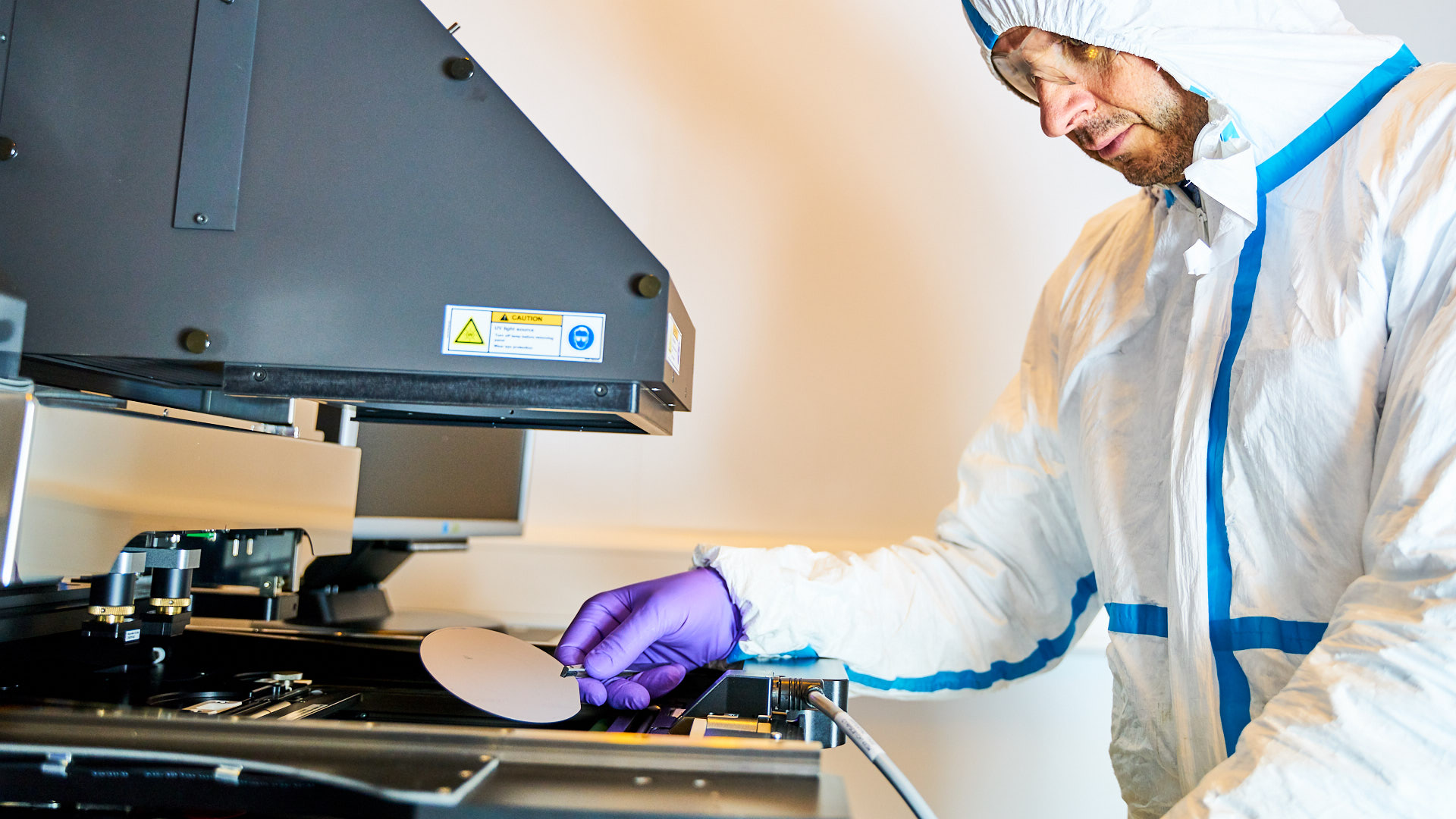
Nanoimprint lithography system
We have an EVG 620 Semi-automated Nanoimprint Lithography System with SmartNIL(TM) tooling for UV-nanoimprint processes. It is capable of imprinting areas from 10 by 10 millimetres up to 150 millimetres in diameter with a guaranteed resolution down to 50 nanometres.
Replication is made by intermediate soft stamps, making it suitable for easy replication from rigid masters such as Si wafers and mask plates.
Displacement Talbot lithography system
We have a PhableR 100M system from EULITHA AG. It is capable of the non-contact, submicron patterning of periodic patterns on areas up to 100 millimetres in diameter.
The theoretical resolution limit is a periodic pitch of approximately 200 nanometres, but the guaranteed pitch is 300 nanometres. The maximum pitch is approximately four microns.
High-aspect ratio resist features are achievable and the machine also has an alignment capability.