Whether we’re developing the solar panels of tomorrow, miniaturising electronics, or finding new ways to power homes, we need to take a close-up look at the materials we’re working with.
Scanning probe microscopy lets us look at specimens right down to the individual atoms they’re made from.
Conventional microscopes use light and magnifying lenses to enlarge specimens so they can be seen by eye, either through a viewfinder or camera. As atoms and molecules are very much smaller than even the smallest light wavelengths, we can’t use light to see them.
Instead, scanning probe microscopes work almost like a record player.
A sharp tip – in some cases measuring just an atom or two across – is moved across the surface of a material. When the tip interacts with the surface - for example, if it detects an electric current - it records the measurement and maps it. As the tip scans the surface, it builds up an image line by line from the measurements, until the features of the entire surface have been recorded.
Depending on the tip used, different properties of the material can be measured, and different images of the surface can be created.
Scanning tunnelling microscopy
Scanning probe microscopy found its feet in the early 80s, with the invention of scanning tunnelling microscopes (STM). Their resolution and function vary, but they all work using the same principle.
Instead of pushing the tip into a surface like a record player needle, the tip is lowered until there is a gap of a single atom’s width between the tip and the surface. When a power source is added, electrons flow down the tip and make a quantum leap across the atom-wide gap. Depending on how close or far away from the surface the tip is, more or less current flows through the circuit. This creates a feedback loop, and the strength of the electric current measured can be used to build up an image of the surface.
Dr Peter Sloan and Dr Kristina Rusimova are taking this technology a step further. Not only are they using the microscope’s electron beam to inspect surfaces, they're also using it to bombard atoms or molecules on them. By exciting molecules (firing electrons at them until some stick), Peter and Kristina can move molecules around and make or break bonds between them.
The team want to understand exactly how this happens and what we can do to control it. They've been putting their theories to the test to understand hot electron transport and single molecule dynamics.
When electrons in a semiconductor are excited with a large amount of energy, they become ‘hot’ and naturally want to lose this energy, fast. In the time taken for them to shed this energy, Peter has discovered the hot electrons shoot sideways a short distance. Measuring this distance has important implications for developing the solar cells of the future.
Solar panels are often made of the semiconductor silicon, and hot electrons are created when light hits them. Electrons are excited with a huge amount of energy and put a lot of this energy into moving a short distance, very quickly. Any energy not lost in this movement is collected and used as green electricity. If we could capture this initial burst of energy as soon as the electrons start moving, solar energy generation could be made far more efficient.
Kristina is also using the technology to manipulate individual atoms and molecules. Instead of looking at how excited electrons move across a surface, she’s using them to create chemical reactions at a molecular level.
This is particularly useful when designing completely novel molecules that don’t exist in nature. By exciting electrons and targeting specific molecular reactions, researchers can develop new drugs and even new materials.
In a UK-first, Kristina also wants to measure the amount of light given off by these reactions. Measuring light emissions would allow researchers to calculate a temporal element to reactions. This adds an extra dimension to the information scanning tunnelling microscopes provide.
Atomic force microscopy
A complementary imaging technique is a variation called atomic force microscopy (AFM). While both use surface probes, atomic force microscopy measures the attracting and repelling forces between atoms to build up an atomic map of the surface.
Where scanning tunnelling microscopy shows us the electronic properties of conductors and semiconductors, atomic force microscopy produces images that more closely reflect the physical structure of materials. As AFM doesn’t rely on the flow of electrons, it also lets us take images of insulating materials at an atomic level.
Dr Adelina Ilie is engineering two-dimensional materials with bespoke properties. In her research, she synthesises 2D nanomaterials inside an ultra-high vacuum instrument. She can then investigate them using scanning probe microscopy without breaking the vacuum in the chamber and exposing them to contamination.
2D materials are stable materials that are a single atom thick. One of the most well-known is graphene, an atom-thick layer of carbon atoms, bonded together in a honeycomb pattern.
Adelina and her team are developing inorganic, graphene-like materials with uses in novel IT and computing systems. One such feature explores 'spintronics'. This is an emerging field that exploits an electron's spin, instead of its charge. Traditional electronics use 3D silicon transistors, which can only be made so small and operate on charge.
Spintronic devices are faster and more energy efficient than their charge-based cousins. This makes them ideal in helping address challenges like the global surge in energy consumption, something only predicted to worsen as new technologies – like Generative AI – become widespread.
When 2D materials are grown on a crystalline substrate, something called a Moiré pattern forms. Like the visual effect of rotating a grid on top of another and creating darker and lighter regions, here, the pattern shows the modulated electron density. Moiré patterns can alter the original properties of the 2D material, and this is something Adelina and her team use to tailor bespoke spintronic materials at the atomic level.
To probe such materials, the scanning tunnelling microscopy technique must be sensitive to the spins localised on the material’s atomic sites. By using all these complementary imaging techniques and in-situ device integration, Adelina can build up a picture of these novel materials and reveal their unique functional properties.
Scanning Hall microscopy
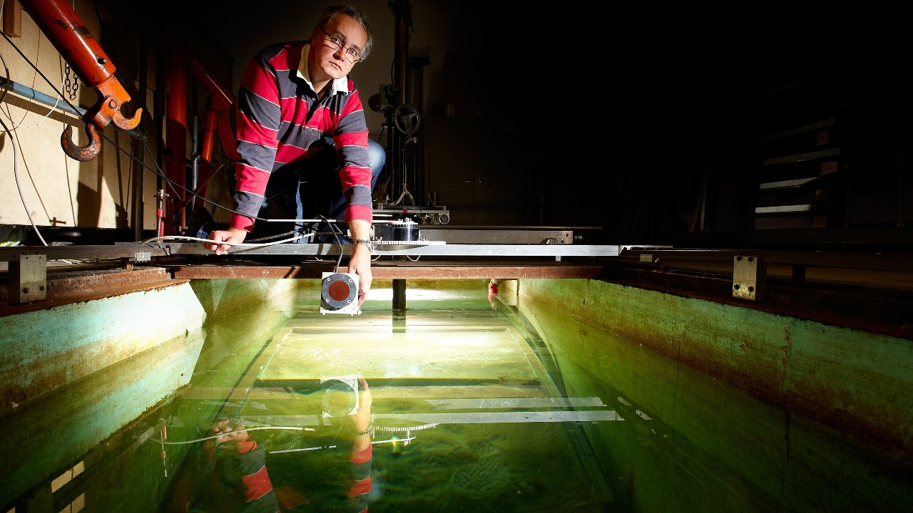
In another area of the department, Professor Simon Bending is also interested in creating new materials with improved properties.
Much like Adelina, he’s using scanning probe microscopy as a feedback tool to learn more about the materials’ properties. Simon, however, is homing in on the magnetic structures in materials to investigate the superconductors of the future.
The technique – scanning Hall microscopy – replaces the sharp tip with a ‘Hall effect’ sensor that detects magnetic fields. Made from a semi-conducting material, it has electrical contacts at either side and a current runs along it. When the sensor encounters a magnetic field, the electron flow bends towards one side or the other. This registers as a voltage at one pair of contacts. As the probe scans the surface of the material, these voltage peaks mark the location of strong magnetic fields, and a magnetic map builds up, line by line.
But what does this have to do with the next generation of superconductors? Superconductors are materials that when below a critical temperature, offer no electrical resistance. In principle, a superconducting wire loop could indefinitely sustain a current with no outside power source.
One of the biggest challenges in superconductor design is maximising the current they can carry while remaining in their unique ‘zero-resistance, zero-dissipation’ state. This all comes down to magnetism. Superconductors repel magnetic fields, but they’re not completely impenetrable to them. All technologically important materials allow magnetic fields to penetrate in the form of tiny nanoscale tubes of flux called 'vortices'. These disrupt the flow of current through the superconductor and reduce their maximum current carrying capacity.
Scanning Hall microscopy allows the team to identify these tiny magnetic defects and tweak the material design to mitigate them. Researchers hope to develop a new generation of superconducting tapes that operate at much higher currents without losses. While still a long way from reality, an electrical grid using efficient superconducting tapes could deliver cleaner, greener power to our homes.
Looking to the future of his research field, Simon believes that scanning probe microscopy as a platform is probably as good as it needs to be, but the innovation lies in the development of new types of sensors that can be placed at the scanning tips.
For the Hall sensors, the team want to make them work more efficiently at higher temperatures. Currently, they only work well at cryogenic temperatures, making them ideal for scanning cold-loving superconductors. But if the team want to investigate ferromagnetic materials at room temperature, there is a clear need for improvement. Graphene sensors are currently being explored to satisfy this need.